 |
|
|
|
The Definitive Betamax Web Resource
|
||
|
|
|
|
The Definitive Betamax Web Resource
|
||
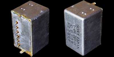
These units are found in the The unit is highly prone to failure causing the florescent display to
go out and the tuner to stop receiving any signals.